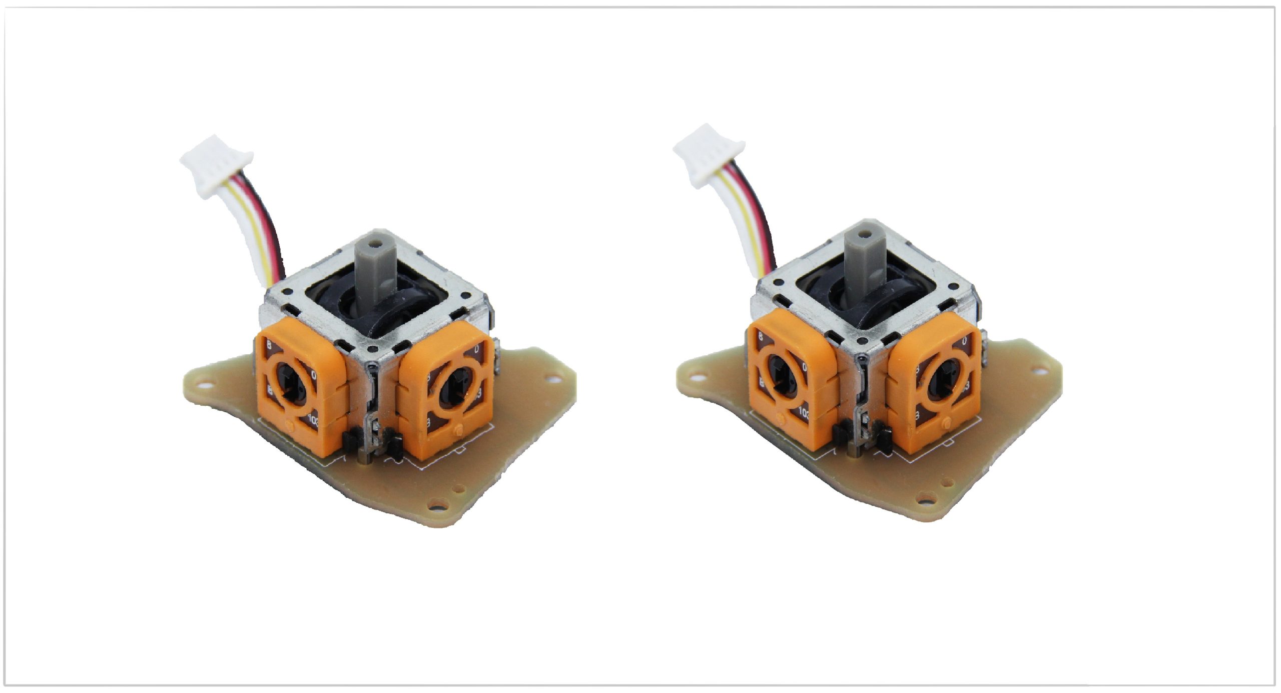
PCBA
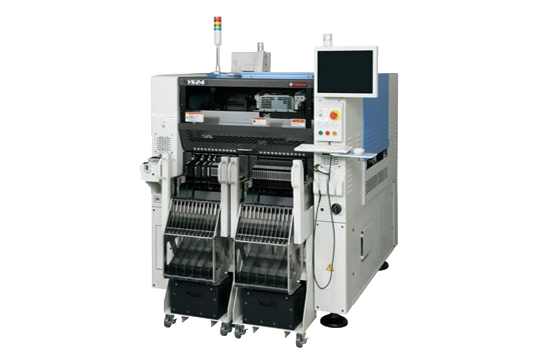
Placement Capability: 72,000/ 39,000/ 28,000 CPH (0.05~1.3sec/CHIP)
Target Components: 01005~55 x 55mm
Placement Accuracy: ± 0.05mm/CHIP
Repeatability Accuracy: ± 0.03mm/ CHIP
Product Capacity: 15 million / year
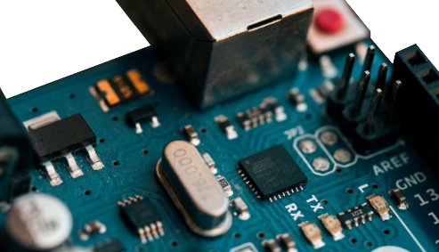
SMT process flow
preparation before production—> solder paste printing/red glue—> patch—> first article inspection—> pre-furnace inspection—> reflow soldering—> AOI inspection—> QC visual inspection—> semi-finished product delivery
Our SMT products cover many fields for many major customers and meet international standards.
The smallest SMT component size can reach 0201
Able to provide 0.6mm*0.3mm~50mm*50mm QFP
0.15mm gap ±0.05 accuracy
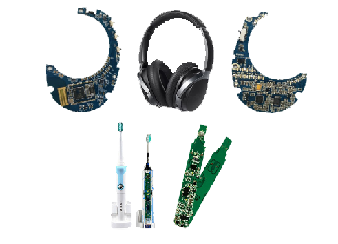
Main applications include:
1. Smart home (wireless headset, smart toothbrush)
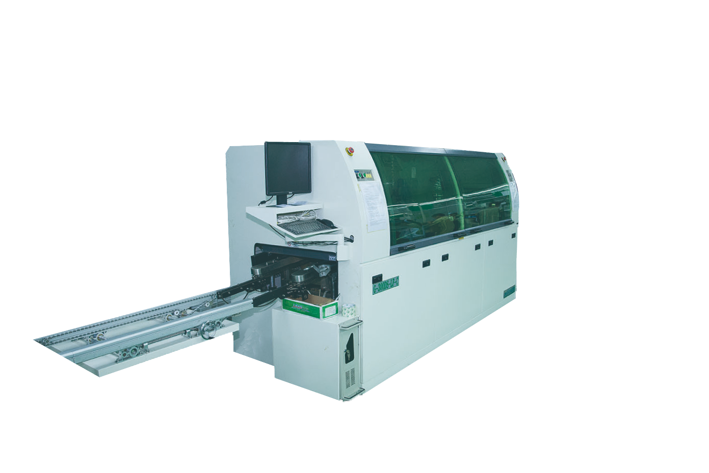
Wave Soldering: Domestic
Capacity: 15 million/year
Power: 90KW Furnace
Temperature Range: 240~300°C
Maximum Card Size: 508*505 mm

Wave soldering process—
PCB board plug-in—>wave soldering furnace—> PCBA height inspection—>Sub-board inspection—-> Sub-board inspection—-> Soldering wire—-> Soldering wire inspection—-> Comprehensive inspection

Our SMT products cover many fields for many major customers and meet international standards.
Main applications include:
- Automotive electronics
(power system, lighting system, sensor)
- Application computer
(computer motherboard)