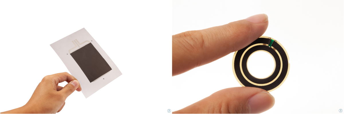
What is thick film printing? Currently, this technology is quite mature and can be printed on a variety of substrates, from high temperature ceramics to common FR4 materials, or polyimide (PI) flexible materials. The resistance value can be from 10 ohm/square to 100K ohm/square (resistance value), the maximum resistance value can reach 100M ohm, tolerance +/- 10%, thick film printing will print on the etched copper outer layer, and in standard convection Cured in an oven, infrared oven or tropical oven, then use laser trimming to adjust the resistance for tight tolerances.
This thick film printing solution makes resistors embedded in printed circuit boards more complex, but more versatile than choosing surface mount passive components. This frees up surface space for more active elements, increasing functionality.
Thick film printing improves the process of embedded resistors by eliminating the need for special termination treatments, such as immersion silver or silver-palladium, gold-palladium, and also speeds up the laser resist trimming process with tighter TCRs; and through stable adhesives The system improves reliability performance. On the other hand, the thick film printing values currently available for testing show good adhesion to clean copper surfaces. This eliminates the need for silver immersion or silver palladium, gold palladium saves costs and reduces concerns about silver migration.
Thick film printing technology can be used to incorporate any combination of fixed resistors, switches, sensors, sliding potentiometers and conductors onto any size, shape, PCB style.